For decades, the solar industry has been defined by the steady, incremental refinement of silicon. The material remains the reliable workhorse of the energy transition, powering the vast majority of photovoltaic installations worldwide. But silicon is approaching a well-known physical constraint: the Shockley-Queisser limit, which caps the theoretical maximum efficiency of a single-junction solar cell at roughly 33 percent. Most commercial silicon panels convert between 20 and 25 percent of incoming sunlight into electricity. Closing the remaining gap through silicon alone has become a problem of diminishing returns.
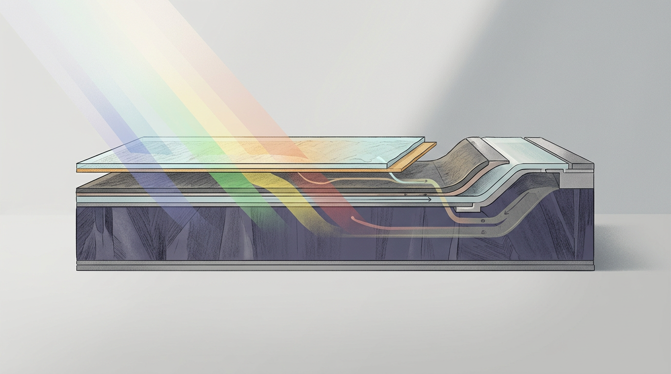
To push beyond that ceiling, researchers have turned to a more complex, layered architecture. A recent milestone highlights the progress of a "triple-decker" design that stacks two layers of perovskite semiconductors onto a base of silicon. Unlike a single-junction cell, which is limited to harvesting a specific portion of the light spectrum, this multi-junction approach allows each material to absorb different wavelengths of sunlight. The perovskite layers are tuned to capture high-energy photons, while the silicon base handles the lower-energy infrared light that would otherwise pass through unused.
Why perovskites — and why now
Perovskites are a class of crystalline materials whose appeal lies in their tunability. By adjusting their chemical composition, researchers can shift the range of wavelengths a perovskite layer absorbs, making them natural partners for silicon in a tandem or triple-junction stack. The materials are also relatively inexpensive to produce compared to other high-performance semiconductors like gallium arsenide, which has long been used in aerospace applications but remains prohibitively costly for terrestrial deployment at scale.
The concept of multi-junction solar cells is not new. Satellite and space-probe designers have used stacked semiconductor architectures for years, achieving efficiencies well above 40 percent under concentrated sunlight. What has changed is the feasibility of bringing a version of that approach to mass-market panels. Perovskite-on-silicon tandems — two-layer designs — have already demonstrated efficiencies that exceed what silicon can achieve alone. The triple-junction configuration extends that logic by adding a second perovskite layer with a different bandgap, carving the solar spectrum into three slices rather than two.
This stacking technique is, at its core, a pursuit of efficiency through density. By extracting more power from the same surface area, triple-junction cells could eventually reshape the economics of both utility-scale solar farms, where land and installation costs matter, and rooftop arrays, where available area is fixed. In markets where space is constrained — dense urban environments, for instance — higher efficiency per square meter translates directly into greater viability.
The durability question
The central challenge remains durability. Silicon panels routinely carry warranties of 25 years or more, a longevity that underpins the financial models of solar deployment. Perovskites, by contrast, are susceptible to degradation from moisture, heat, and prolonged UV exposure. Early perovskite cells lost performance rapidly under real-world conditions, and while encapsulation techniques and compositional improvements have extended their operational lifetimes considerably, no perovskite-based product has yet demonstrated the multi-decade reliability that silicon delivers as a matter of course.
Manufacturing scalability presents a separate set of obstacles. Laboratory-scale cells are produced under tightly controlled conditions that do not translate automatically to high-throughput factory lines. Achieving uniform perovskite films across large areas, maintaining consistent performance from cell to cell, and integrating three distinct semiconductor layers without introducing defects at the interfaces — each of these steps adds complexity that the industry has not yet resolved at commercial scale.
The trajectory, however, is clear in its direction if not its timeline. Each successive efficiency record narrows the gap between what multi-junction architectures achieve in the lab and what would be required to justify the added manufacturing cost. Whether the triple-junction design becomes the dominant architecture of the next decade or serves primarily as a proving ground for perovskite integration, it represents a structural shift in how the field thinks about solar conversion — not as a single-material problem, but as an engineering challenge of spectral optimization across layers. The question is no longer whether stacked designs can outperform silicon alone, but whether they can do so durably and affordably enough to displace it.
With reporting from Nature News.
Source · Nature News